Memory Chip: The Key to Smart Connectivity

Making Memory Chips – Process Steps
Catalog |
Edge Computing and memory chips
The most important factors driving the development of artificial intelligence are computing power, algorithms, and data, respectively. That is changes in computing technology, innovation in theoretical algorithms, and the generation and accumulation of massive amounts of data. No matter how advanced the algorithm progresses, or how powerful the arithmetic power improves, in the final analysis, it is necessary to calculate, carry and store a large amount of data.
Especially with the continuous rise and development of autonomous driving, 5G, smart home, and other such IoT-related technologies, coupled with the dramatically increasing demand for remote communication and collaboration brought about by the global epidemic, so there will be more and more data generated continuously. Some have also compared data to oil in the age of artificial intelligence. This also places more stringent demands on both the performance and efficiency of data processing.
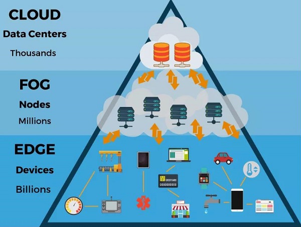
Usually, the data center is the main battlefield for processing these data, where there are thousands of servers and massive hardware resources for data computation transmission and storage. But as the volume of data grows rapidly, it puts great pressure and challenges on the computing power of the chips, the bandwidth of the network, and the capacity of the storage in the data center.

edge computing and IoT applications
It is slowly becoming impossible to transfer all the data to the data center, process it, and then send it out. In fact, less than 1% of the data generated by the aforementioned sources is processed efficiently. So people consider whether they can process the data directly where it is generated so that they can largely reduce the bandwidth of transmission, storage space, and computational pressure. This is the main background of the rise of edge computing, that is, computing at the edge of the data processing network.
One of the important application scenarios of edge computing is IoT applications. For IoT, it is initially just some sensors, data sending and receiving devices, and some simple controller MCUs and so on. But as the amount of data increases, the demand for the computing power of these IoT devices is getting bigger and bigger, but this is only one side.
Another important aspect is that these IoT devices also have very strict limitations on cost and power consumption. For example, for wearable devices, we not only want it to be able to run various applications smoothly, collect and sense various data of our movement and physiology but also to be power-saving enough, preferably to be charged once a week or once a month.
Therefore, for IoT hardware devices, high energy efficiency, low power consumption, and small size will be the future development direction of such devices and chips. It is worth noting that the chip here includes not only the processor, but also those data transmission modules, sensor modules, and, very importantly, the storage unit, especially the system RAM memory.
New storage technology for IoT and AIoT
For processors, many MCUs have been able to achieve a good balance between power consumption and performance, but the technological progress of storage units is not so obvious.

memory chip
The most common SDRAM was released around 1994 when the semiconductor process node was still at 800nm. pSRAM was born around 2005, corresponding to the 90nm process node, and then the low-power SDRAM was released in 2007 when the process node was 65nm. Then it seems that the definition of standards regarding DRAM stagnated. As you can see, there is a relatively large gap and the chasm between the standards and processes of the two types of chips, mobile device processors and memory.
In order to keep filling this gap, the industry introduced a technology called HyperBus in 2014 and made an update in 2019. HyperBus is essentially an interface technology, and the most important feature of HyperBus is the small number of pins compared to other memory's transmission control interfaces, which allows for a cleaner and smaller area when designing the circuit.
The HyperBus technology-based memory chip is called HyperRAM, which has only 13 pins compared to traditional RAM products that have 3 to 40 pins. This greatly simplifies the PCB design on the one hand, and also allows more flexibility in MCU selection. For example, we can use the extra pins on the MCU for other things, or we can simply choose an MCU with fewer pins, thus reducing costs.

HyperRAM
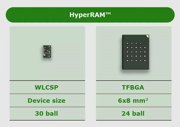
Another benefit of the reduced pin count of HyperRAM is the ability to use smaller package sizes, such as consumer-oriented HyperRAM packages up to wafer-level chip packages, with some package options shown below.
For automotive and industrial applications: 24-ball 8mm x 6mm TFBGA
For consumer products: 49-ball 4mm x 4mm WFBGA
For lean size requirements such as IoT: 15-ball wafer-level chip package (WLCSP)
Good bare wafer (KGD)
Using smaller packages can further reduce PCB size, which is very important for wearable consumer devices such as smart watches, smart bracelets, etc...
In addition to the area, power consumption is also critical for IoT devices. For example, many IoT devices are battery-powered. Many devices are even very difficult to change the battery, such as those deployed in mines, oil and gas fields, chemical plants, and other dangerous environments. So the power consumption of these IoT devices directly determines their working life.
Security of AIoT memory chip
We may be familiar with the hacking of personal computers or data centers, but what most people may not know is that IoT devices are also very vulnerable to cyber-attacks. In 2019, for example, the number of cyberattacks launched against IoT devices in the United States jumped 300 percent year-over-year.
To make matters worse, about 57% of IoT devices have difficulty resisting these attacks. For example, a significant number of attacks are targeting devices like smart meters and smart gas meters to modify the readings of these meters so that they can underpay or not pay for their energy usage. There are also many attacks on medical devices and wearable areas to illegally access and collect users' private information, etc. It is important to understand that the damage caused by these attacks is huge. Some data show that the average cost of each attack is $9 million.
From the hardware point of view, the main places where these security vulnerabilities exist are the processing unit itself and the external flash memory that stores critical program code or data. In the case of simpler wearable products or IoT products, security issues mainly arise in the control chip, such as the lack of complex cryptographic algorithms, differential power analysis, key encryption storage, and so on.
As these IoT devices continue to evolve, the control chip becomes more and more complex, with more and more programs to run, and moving towards a chipless memory process. At this point, embedded memory is not enough or even exists and external flash memory must be used to store program code. However, if such external flash memory lacks the necessary security features, it can become a major security vulnerability for the system.
To address such security issues, a common practice is to replace external NOR Flash in IoT devices with Secure Flash, which, by its very nature, provides secure storage space with basic encrypted authentication, thus allowing only authorized hosts to perform read and write operations.
In fact, in addition to secure authentication, other hardware protection features are required to better defend against many types of cyberattacks.
For example, the system recovery feature detects potential attacks and automatically reboots the device after an attack has occurred, and executes known security codes. And the secure channel feature enables remote firmware updates so that even if the control unit is compromised, the memory can upgrade the bootloader code to a secure version without the control unit's intervention. This allows the host to be forced into a clean boot mode using a known security code.
It is also worth noting that secure flash memory is typically packaged in the same size and pin locations as standard flash memory and is controlled through the standard SPI NOR Flash command set, which further facilitates the use of secure flash memory.
Summary
In the current era of data blowout, memory chips are of increasing importance. Especially in edge computing and IoT applications, the performance, power consumption, and size of the memory chip are all critical evaluation and consideration factors.
1.What are memory used in IoT devices?
Traditional External Flash Memory: Many consumer products use this type of memory, because it is inexpensive, reliable, and flexible, offering a high degree of density and the ability to execute in place without using too much power. Flash memory falls into two categories: NOR Flash and NAND Flash.
2.What is chip in IoT?
IoT modules or chips are technically identified as electronic devices that are embedded in machines, objects, and things, capable of connecting to wireless networks and sending and receiving data. These devices operate on different protocols, such as NB-IoT, LTE, and BLE 5.0, among others.
 How to Use an External Hard Drive?UTMEL24 June 20218992
The external hard drive is a compact and portable hard drive storage which can be plugged in or unplugged at any time. It mainly uses USB or IEEE1394 interfaces. It can transmit data with the system at a higher speed. The IEEE 1394 interface transfer rate is 50-100 MB/s.
Read More Introduction to RAID (Redundant Arrays of Independent Disks)UTMEL01 July 20218584
RAID (Redundant Arrays of Independent Disks) means "a redundant array composed of independent disks". The RAID is the combination of many independent disks that combined into a large-capacity disk group. It uses the bonus effect of individual disks to provide data to enhance the performance of the entire disk system.
Read More What is NAND Flash?UTMEL04 November 202111370
NAND Flash is a better storage device than hard disk drives and is particularly evident in low-volume applications up to 4GB. As the quest continues for lower power consumption, lighter weight, and better performance, NAND is proving to be very attractive. Its development goal is to reduce the cost per bit of storage and increase storage capacity.
Read More Memory Chip: The Key to Smart ConnectivityUTMEL03 November 20212572
In today's post, we talk about memory chips, especially their emerging applications in the AIoT smart interconnect space.
Read More Emerging Storage Technologies: MRAM, RRAM, and PCRAMUTMEL08 January 202611491
The semiconductor industry is turning to emerging memories that offer higher storage performance, lower cost, and the ability to move toward process miniaturization. Three of these memories stand out -- MRAM, RRAM, and PCRAM.
Read More
Subscribe to Utmel !


 Product
 Brand
Brand Articles
 Tools
Tools


